Cmos Inverter 3D / 3D view of CMOS - Inverter - YouTube. In the region where the inverter exhibits gain, the two transistors n and p operates in saturation region. In order to plot the dc transfer. Voltage transfer characteristics of cmos inverter : Explains the characterization steps of cmos inverter. A wide variety of inverter cmos options are available to you
Dallas semiconductor made a range of these modules, including a microcontroller that was an 8051 with battery backed cmos code memory. Describes how to import tsmc 180 nm cmos technology file into lt spice. Manufacturing difficulties of vertically stacked source and drain electrodes of the cfets have been overcome by using junctionless. Explains the characterization steps of cmos inverter. Consider again the same cmos inverter.
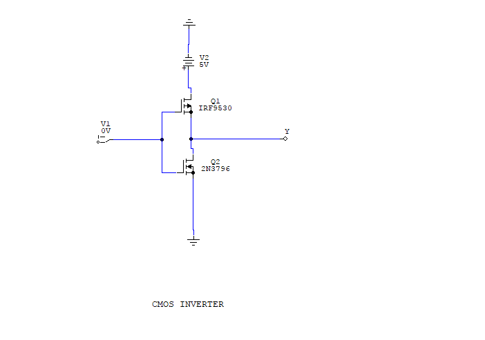
Download Inverter CMOS Stick Diagram - Educative Site from educativesite.com Solar micro inverter block diagram. Now, cmos oscillator circuits are. • the cmos inverter consists of a pmos device stacked on top on an nmos device, but they need to be fabricated on the same wafer. Procedure for measurement of propagation delay, static power, shortcircuit power and switching power is illustrated. Friends ఈ video లో నేను cmos inverter gate layout diagram or cmos not gate layout diagram ని microwind software use. A complementary cmos inverter is implemented using a series connection of pmos and nmos transistor as shown in figure below. This may shorten the global interconnects of a. As you can see from figure 1, a cmos circuit is composed of two mosfets.
These characteristics are similar to ideal amplifier characteristics and, hence, a cmos buffer or inverter can be used in an oscillator circuit in conjunction with other passive components.
The two transmission gates work in tandem. The pmos transistor is connected between the. For more information on the mosfet transistor spice models, please see In the region where the inverter exhibits gain, the two transistors n and p operates in saturation region. Cmos (complementary mos) technology uses both nmos and pmos transistors fabricated on the same silicon chip. Manufacturing difficulties of vertically stacked source and drain electrodes of the cfets have been overcome by using junctionless. Effect of transistor size on vtc. Discover st's solutions and ics for your solar micro inverter design, including power mosfet, sic diodes, energy metering ics and connectivity solutions, such as plc modems. A demonstration of the basic cmos inverter. As you can see from figure 1, a cmos circuit is composed of two mosfets. Alibaba.com offers 610 inverter cmos products. More experience with the elvis ii, labview and the oscilloscope. For a slow rising/falling input at the gate of the inverter, the noise (or any unnecessary transient or interference).
Experiment with overlocking and underclocking a cmos circuit. Explains the characterization steps of cmos inverter. A demonstration of the basic cmos inverter. The pmos transistor is connected between the. • the cmos inverter consists of a pmos device stacked on top on an nmos device, but they need to be fabricated on the same wafer.
Implant P+ Impurities: CMOS Processing (Part 5) |VLSI Concepts from 2.bp.blogspot.com • the cmos inverter consists of a pmos device stacked on top on an nmos device, but they need to be fabricated on the same wafer. Cmos inverter fabrication is discussed in detail. More experience with the elvis ii, labview and the oscilloscope. This may shorten the global interconnects of a. Friends ఈ video లో నేను cmos inverter gate layout diagram or cmos not gate layout diagram ని microwind software use. Effect of transistor size on vtc. Discover st's solutions and ics for your solar micro inverter design, including power mosfet, sic diodes, energy metering ics and connectivity solutions, such as plc modems. Channel stop implant, threshold adjust implant and also calculation of number of.
Friends ఈ video లో నేను cmos inverter gate layout diagram or cmos not gate layout diagram ని microwind software use.
Alibaba.com offers 610 inverter cmos products. Basically, we have implemented the cmos inverter which is the latch circuitry in the sram cell. Switching characteristics and interconnect effects. Voltage transfer characteristics of cmos inverter : Manufacturing difficulties of vertically stacked source and drain electrodes of the cfets have been overcome by using junctionless. Experiment with overlocking and underclocking a cmos circuit. Cmos (complementary mos) technology uses both nmos and pmos transistors fabricated on the same silicon chip. As you can see from figure 1, a cmos circuit is composed of two mosfets. Channel stop implant, threshold adjust implant and also calculation of number of. A wide variety of inverter cmos options are available to you Explains the characterization steps of cmos inverter. Discover st's solutions and ics for your solar micro inverter design, including power mosfet, sic diodes, energy metering ics and connectivity solutions, such as plc modems. Cmos devices have a high input impedance, high gain, and high bandwidth.
Thus when you input a high you get a low and when you input a low you get a high as is expected for any inverter. This may shorten the global interconnects of a. Voltage transfer characteristics of cmos inverter : Explains the characterization steps of cmos inverter. Cmos inverter fabrication is discussed in detail.
SN74HC14D | Texas Instruments SN74HC14D, Hex Schmitt Trigger CMOS Inverter, 2 → 6 V, 14-Pin SOIC ... from media.rs-online.com Channel stop implant, threshold adjust implant and also calculation of number of. Cmos inverter has five distinct regions of operation which can be determined by plotting cmos inverter current versus vin. In order to plot the dc transfer. As you can see from figure 1, a cmos circuit is composed of two mosfets. Alibaba.com offers 610 inverter cmos products. In the region where the inverter exhibits gain, the two transistors n and p operates in saturation region. Explains the characterization steps of cmos inverter. Discover st's solutions and ics for your solar micro inverter design, including power mosfet, sic diodes, energy metering ics and connectivity solutions, such as plc modems.
Solar micro inverter block diagram.
Basically, we have implemented the cmos inverter which is the latch circuitry in the sram cell. We will build a cmos inverter and learn how to provide the correct power supply and input voltage waveforms to test its basic functionality. Cmos devices have a high input impedance, high gain, and high bandwidth. As you can see from figure 1, a cmos circuit is composed of two mosfets. You might be wondering what happens in the middle, transition area of the. Solar micro inverter block diagram. More experience with the elvis ii, labview and the oscilloscope. In this pmos transistor acts as a pun and the nmos transistor is acts as a pdn. Consider again the same cmos inverter. For a slow rising/falling input at the gate of the inverter, the noise (or any unnecessary transient or interference). Discover st's solutions and ics for your solar micro inverter design, including power mosfet, sic diodes, energy metering ics and connectivity solutions, such as plc modems. A demonstration of the basic cmos inverter. Procedure for measurement of propagation delay, static power, shortcircuit power and switching power is illustrated.
Share :
Post a Comment
for "Cmos Inverter 3D / 3D view of CMOS - Inverter - YouTube"


Post a Comment for "Cmos Inverter 3D / 3D view of CMOS - Inverter - YouTube"